Via In Pad Fr4 PCB


Via In Pad fr4 pcb board, using copper plating or epoxy to fill holesfor circuit board factor, prevent solder paste or flux from flowing into the via in pad, avoid solder ball getting into via or solder mask cover on pad and cause false soldering. HUIHE CIRCUITS Via In PadPCBhas passed ISO9001/ISO13485/IATF16949/UL/RoHS/REACH certification.
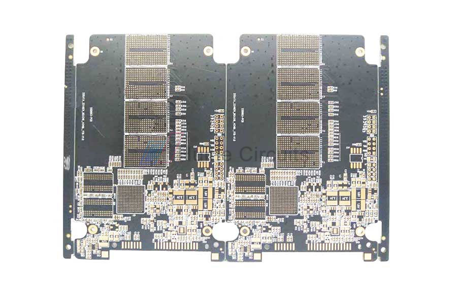
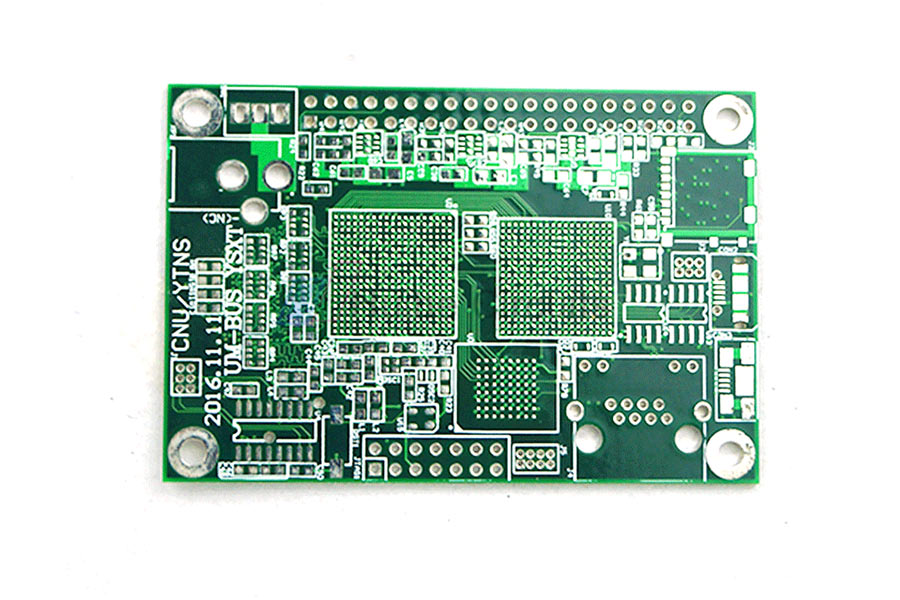
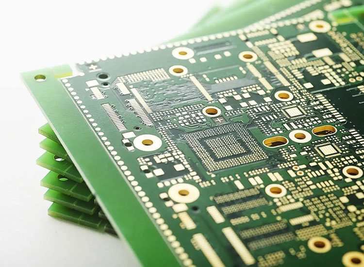
Via In Pad Fr4 PCB List
10 Layer Impedance Control Resin Plugging PCB
16 Layer ENIG Press Fit Hole PCB
6 Layer ENIG via-in-pad Prototype PCB Board
6 Layer ENIG via-in-pad PCB Prototype Service
6 Layer ENIG via-in-pad PCB
8 Layer ENIG via-in-pad PCB
What Is A Hole-In-The-Panel Circuit Board?
The hole in the disk is an important part of the multi-layer PCBChina. It is not only responsible for the main functions of the PCB, but also the cost of drilling usually accounts for 30% to 40% of the fr4 circuit board manufacturingcost. In short, the holes pressed on the pads on the PCB can all be called holes in the disk.
Processing Requirements For Hole Plugs In The Disk
No solder mask ink entering the hole
There should be no tin beads hidden in the hole
No explosive oil, ink pads, making it difficult to mount components, etc.
Common Sense Of PCBCircuitBoard Plug Hole
Prevent the tin from penetrating the component surface from the via hole to cause a short circuit when the PCB is wave soldered
Avoid flux residue in the vias
Prevent the tin balls from popping up during wave soldering, causing short circuits
Prevent surface solder paste from flowing into the hole, causing false soldering and affecting placement
If you want to know more about pcb board material fr4and fr4 pcb thickness, please contact us.
Send product request
Other supplier products
 |
2 Layer Rogers ENIG PCB | Number of layers: 2 size: 98.45*49.45mm Surface finish: ENIG Base material: Rogers 4350B Min. hole diameter: 0.5mm Minimum Line Width:/mm Minimum L... |
 |
Heavy Copper PCB | Heavy Copper PCB, pcb fabrication up to 12oz, large current, pcb fabrication base material is FR4/Teflon/Ceramic, pcb fabrication used in high-powe... |
 |
2 Layer Rogers ENIG Rf PCB | Number of layers: 2 size: 96.45*87.73mm Surface finish: ENIG Base material: Rogers 4350B Min. hole diameter: 0.5mm Minimum Line Width:/mm Minimum L... |
 |
Blind Buried Vias & Hdi Pcb | Blind & Buried Via Board, use micro blind vias to increase the trace distribution density. Improve radio frequency, electromagnetic wave interf... |
 |
2 Layer Rogers LF-HASL PCB | Number of layers: 2 size: 184.2*158.9mm Surface finish: LF-HASL Base material: Rogers 4350B Minimum Line Width: 0.227mm Minimum Line Space: 0.... |
Same products
 |
PCB Surface | Seller: GreensTone (Shenzhen) Electronics Co., Limited | PCB surfacefinish include: PCB plating finishesis a coating between a component and a bare board ... |
 |
PCB Components Sourcing | Seller: GreensTone (Shenzhen) Electronics Co., Limited | GreensTone Electronics employs a dedicated, parts sourcing and procurement team to manage the log... |
 |
PCB Capability | Seller: GreensTone (Shenzhen) Electronics Co., Limited | GreensTone has successfully served customers with pcb manufacturing capabilitiesservice in commun... |
 |
PCB Assembly Service | Seller: GreensTone (Shenzhen) Electronics Co., Limited | GreensTone specializes in the pcba pcb assembly, including: Circuit board assembly Surface moun... |
 |
High-TG PCB | Seller: GreensTone (Shenzhen) Electronics Co., Limited | Glass Transition Temperature is referred to as Tg, and FR4 is a designation for a particular type... |